
![[Inglese]](images/italy.gif)


PCMCIA GPS Time Receiver
Questa pagina è disponibile esclusivamente in inglese
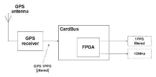
The goal of the current task is provide an accurate 10MHz square wave to manage the switches with the development of a FPGA card.
In the previous TestBed configuration the 10MHz square wave was provided by the Tekelec or Symmetricom devices. In the actual configuration, the step to produce the 10MHz signal is provided with the following steps that are summarized in the Figure 1:
- the GPS signal is received by a GPS receiver(details here);
- the GPS receiver provides a 1PPS (1 Pulse Per Second) signal;
- the 1PPS signal is the input of a FPGA that provides a 10MHz square (duty cycle 50%) wave.
|
| Figure 1: Block diagram for generation of 10MHz square signal. |
The GPS receiver supplies the development card with the GPS time pulse signal: it generates one pulse (100μs long) per second UTC (Coordinated Universal Time), a high precision atomic time standard. This signal is given as input to FPGA card that performs a frequency division to obtain the output wave.
Several acquisitions revealed that the signal provided by the GPS receiver is jitter-affected. For this reason the FPGA is programmed to carry out a filtering operation on the input signal to reduce the effects of the noise.
The so obtained 1PPS signal is then used as reference for the generation of the high precision 10MHz square wave, which in turn constitutes the input of another device generating a 10KHz square wave, used to control the multi-terabit/s switch. Due to the high speed of the system, the 10KHz wave jitter has to be lower than 1μs.
1- Frequency divider
The idea that lays at the base of the whole system is really simple and can be summarized by the Figures 2, 3, and 4.
|
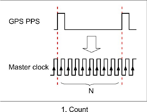
| Figure 2: How the counter works. |
|
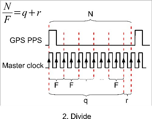
| Figure 3: How the divider works. |
|
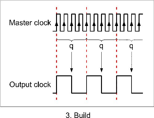
| Figure 4: How the final output is built. |
From the GPS receiver the system obtains the basic timing reference from which it is possible to build the output: the high accuracy 1PPS signal, whose precision we can’t query. During the ith cycle, delimited by the rising edge of two consecutive pulses, the clock internal to the device is used to measure the pulse length (so a counter is needed, counting the number of clock cycles present in a 1PPS period) which should be close to the ratio between the internal clock’s frequency and the reference signal’s frequency (Figure 2). The obtained value is then divided by the ratio between the wanted output signal frequency (let it be a generic frequency F) and the reference signal frequency (i.e. 1Hz) in order to get the output’s signal length (measured in clock cycles) (Figure 3). This value is used to build the F[Hz] square wave during the (i + 1)th 1PPS cycle, supposing the internal clock’s frequency to be stable (Figure 4). The stability assumption has to not to be taken for granted for long, so the procedure has to be repeated continuously, for every incoming pulse. In this way it is possible to to put bounds on the effect of the frequency drift affecting the quartz oscillator included on the FPGA.
Another aspect that needs to be considered for a proper functioning is the presence of the reminder in the division calculation, representing the fraction of Master Clock cycle lost in the output generation. If the output is built without considering it, high bad synchronization risk has to be taken into account. However, the reminder can be recovered during the generation phase through the use of an accumulator that keeps track of the fractions of Master Clock cycles lost, allowing to compensate the distortion everytime the accumulated fractions reach the unity value by extending the square wave period for one additional Master Clock cycle.
2- Jitter
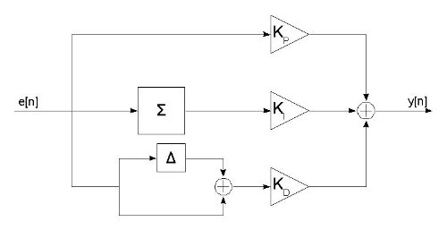
The filtering of the jitter was achieved with a PI controller (Figure 5).
|
| Figure 5: Block diagram of PI controller. |
Its mechanism is: it takes the last measured value of the GPS-1PPS input signal and compares it with the length that is stored in memory. The difference between them (called error signal) is then used to adjust the same 1PPS output length with further two contributions, whose initials form the name of the controller:
- P: a proportional one, obtained multiplying the last error by the correspondent weight KP. Conceptually, its task is to handle the intrinsic drift affecting the digital system;
- I: an integral one, obtained accumulating the error multiplied by the correspondent weight KI. Its purpose is to adjust the output 1PPS length in case the oscillator’s frequency changes.
Usually, also a derivative part should partecipate to the control with a predictive task, but in our case its contibution is not helpful: the reason could be identified with the fact that jitter (which is a random noise) affects the reference signal, and the use of a derivative dependent component leads to unwanted fluctuations.
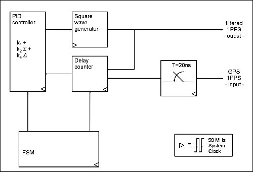
A block scheme of the FPGA implementation of the controller is given in Figure 6, where the FSM (Finite State Machine) is the component the coordination of the various blocks is delegated to.
|
| Figure 6: Block diagram of PI controller. |
|
Pages hosted by "IP-FLOW Group" - DIT - Università di Trento - Italy. © IP-FLOW Project 2004, All Rights Reserved. Last updated: 2008-09-10 05:37:04 |