Porting to all FPGA-PCMCIA
Questa pagina è disponibile esclusivamente in inglese
The goal of the activity is to reduce the size of the system and its complexity.
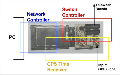
This activity involves of three funcitonalities in a single PCMCIA device that is based on a FPGA card.
- GPS Time Receiver
- This part receives the GPS signal with the current time and generates two accurated one at 1Hz frequency and one at 10MHz frequency.
- Network Interface
- This part provides the interconnection between the PCMCIA and the PC that manages the system. The part intercats with the GPS Time Receivere to obtain accurated clock for the syncronization.
- Switch Controller
- This part provides the management of the optical switch boards. It also intercats with the GPS Time Receivere to obtain accurated clock for the syncronization.

|
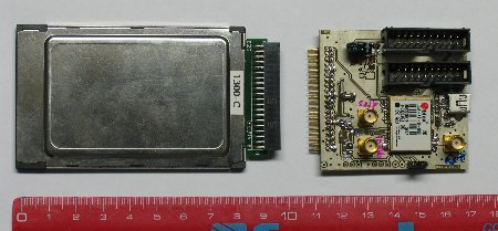
| Prototype of PCMCIA and GPS receiver |

|
| Prototype of with block funcitonalities and connections |
|
Pages hosted by "IP-FLOW Group" - DIT - Università di Trento - Italy. © IP-FLOW Project 2004, All Rights Reserved. Last updated: 2008-09-10 05:37:05 |
![[Inglese]](images/italy.gif)


